 [via newscientist]
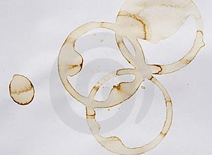
THE rings left behind by spilled coffee have inspired a new way to make ultrathin coatings for LCD and plasma flat-screens.
In LCDs, transparent conductive coatings are used to form an electrode on the surface of the screen, while in plasma TVs they provide a shield that prevents electromagnetic fields from straying. The traditional techniques for making such coatings include sputtering a fine layer of indium tin oxide onto the surface. ITO is highly conductive and transparent to visible light, but the process is expensive, requiring clean rooms and vacuum chambers.
Ivan Vakarelski at the Institute of Chemical and Engineering Sciences in Singapore realised that coffee stains could point the way to a cheaper alternative. Spill coffee and the evaporating liquid drives coffee particles to the edges of the spill - which ultimately produces the circular stain. The coffee granules are being "assembled" by the varying evaporation and convection rates in the fluid. Vakarelski and his colleagues figured that if they could mimic the process in a controlled fashion, they could create a pattern of granules of other materials to form a nanoscale conductive coating.
Instead of coffee, they started with a suspension of gold particles, each about 20 nanometres across. The suspension was left to dry on a glass plate covered with closely packed latex microspheres, each about 50 to 100 micrometres in diameter.
By adding suitable surfactants and lowering the temperature to 4 °C, the team was able to control the evaporation and convection rates, causing the gold particles to move to the base of the latex balls where they settled to form rings and bridges. Once the liquid had evaporated, they were left with a network of connected gold nanoparticles (Physical Review Letters, vol 102, p 058303).
"Our gold network is finer than spider's silk and is also conductive," says Vakarelski. He reckons that gold nanonets could make even better conductors than ITO coatings.
The team has made coatings a few square centimetres in size in the laboratory and aim to increase this tenfold. Unlike many new technologies, the nanonet process will be easy to scale up, says Vakarelski.
The work has "considerable merit", says Jennifer Lewis at the University of Illinois at Urbana-Champaign, an expert on the self-assembly of nanoparticles. "A key advantage of their approach is that the resulting networks are semi-transparent and their density can be tuned by varying the size of the [latex-microsphere] template."
Found this Post interesting? Receive new posts via RSS (What is RSS?) or subscribe via email at the top of this page...


